The Video Terminal
When you read the description of the Video Terminal below you will probably learn to appreciate the "random" in Random Access Memory a little more. Why? RAM memory was very expensive back in '76, therefore Steve decided to use a shift register instead to be used as video memory. Obviously this had an enormous impact on the behaviour of the Video Terminal. But still, the Apple 1 was the first "personal computer" with a built in Video Terminal, therefore it was still a lot better than its competitors.
After some browsing on the internet I found that Steve probably has been inspired by the TV Terminal, designed by Don Lancaster's TV Terminal somewhere around 1973.
This TV Terminal could display 2 pages of 16 lines with 32 characters and was often used as a "cheap" terminal for the Altair 8800.
The way I see it the Apple 1 terminal is an improved version of the TV Terminal.
For example the TV Terminal could not scroll, at the end of the page the cursor simply returned to the top of the screen.
And the Apple 1 Terminal can display more lines and more characters per line.
I will try to explain the most important properties of the Apple 1 Video Terminal in detail.
I shall not explain all features of the Video Terminal though.
Not only would it take me at least another week to study the schematics in order to understand it all, it would also take me another month to explain it all.
The result would be a very long and dull explanation anyway.
Of course you can study the diagram yourself if you want to know exactly how it all works.
The diagram is included at the end of the Apple 1 User Manual, which can be downloaded from the downloads section.
Block Diagram
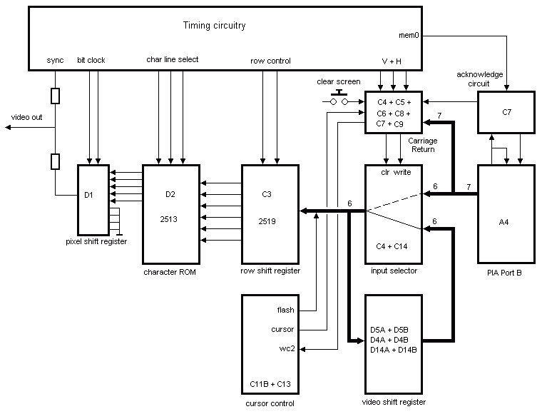
That's quite something, isn't it. Well I'll try to explain most of the blocks in the block diagram in more detail below. One thing I will not explain is the Timing Circuitry. It consists of half a dozen counters, counting pixels, lines, H and V pulses, etc. I will try to explain the other blocks though.
B.T.W. In the downloads section you'll find the data sheets of the 2504, 2513 and 2519, in case you are interested in the details about these very special chips.
Hang on to your hat, here we go:
The Video Shift Register
The very heart of the circuit is probably the shift register, therefore I'll start there.
This shift register replaces the more traditional video RAM memory and is responsible for holding all the characters which are visible on the screen.
How many?
Well 24 rows of 40 characters each, which are 960 characters.
The shift register can hold 1024 characters, which means that we've got 64 characters to spare.
A total of 6 shift register of the type 2504 are used to hold 6 bit wide words.
Why only 6 bits?
You'll see when we discuss the character generator circuitry.
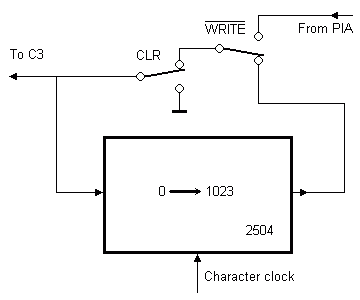 This simplified representation of one of the shift registers shows you the actual operation.
Both "switches" are part of ICs C4 and C14.
In normal operation both switches are in the drawn position, allowing the shift register to run around in circles endlessly.
This means that all characters remain on the screen where they are.
The currently "exposed" character is fed to C3 to be displayed.
When a new character is to be entered into the carousel we have to wait for the character "under the cursor" to pass by, only then can we assert the WRITE signal which flips the right switch to accept the new character. Immediately after that the switch is again returned to its original position and from then on the new character will circulate in the carousel, effectively replacing the character which used to fill that space previously.
Do you know now why RAM is called Random Access?
With RAM you wouldn't have had to wait for the character to appear before it can be replaced.
This hopefully explains why the Apple 1 display is updated so slowly, the processor has to wait a full cycle of 16.7ms each time before it can update the next character.
There's one more switch there, what does that one do? Well effectively it clears the display memory. There are actually 3 sources which can clear the memory:
- The Clear Screen switch. Sounds obvious, but did you know that if you press the switch shorter than 16.7 ms you can partially erase the screen? Simply pressing it longer than 16.7 ms will erase the entire screen (several times).
-
During Vertical Blanking Interval the 64 "non visible" characters of the carousel are erased.
Remember them?
We've got 1024 locations and need only 960 of them, 64 are not visible.
If they were not erased old display contents would scroll in from the bottom of the screen. Therefore the 64 spare characters are erased during VBI. - Last but not least a line is filled with blank characters until the end of the line whenever a Carriage Return is printed. We don't actually need to fill the line with blanks, the line was blank already, but we do need to advance the cursor to the first position of the next line and this is the only easy way to do it.
Please note that the Character Clock is not a constant clock signal. It is only clocked when the appropriate characters must be made visible. This means that most of the time the clock is not active, only when a line of 40 characters is needed a burst of 40 pulses is applied to the Character Clock line.
Carriage Return Circuit
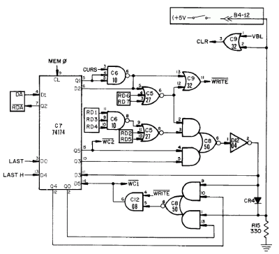 This automatically brings us at the Carriage Return Circuit.
The purpose of this circuit is to control the CLR switch in the shift register circuitry in such a way that the line is filled with blanks until we reach the first character of the next line.
At the same time the same circuit is responsible for creating the WRITE signal for the same shift register circuit.
This circuit is rather complicated and I don't pretend to understand it all. Like I said understanding it all would take me at least another week, and it wouldn't really bring much news. A general understanding of the principles behind the Apple 1 is quite enough for me.
In the upper right corner you see the Clear Screen key and the VBL line connected to an OR gate, which controls the CLR switch of the shift register circuitry we saw above.
This same OR gate is also controlled by the inverter D12 via the diode you see at the bottom of the screen.
This is the clear signal which is generated by printing a carriage return.
The LAST en LAST H lines in the left hand corner tell the circuit when the end of the line is reached.
Somewhat hidden in the center of the screen you'll see all the 7 lines coming from the PIA (RD1 to RD7, which represent b0 to b6 of the ASCII output).
This circuit fully decodes a Carriage Return character ($0D).
The WC2 line, which may be hard to find in the diagram, is the signal to the Cursor Control circuitry to advance the cursor one position.
Acknowledge Circuit

The clipping above shows the acknowledge circuitry.
Its purpose is to signal the acceptance of the character by the terminal to the software.
You won't find the circuit as it is drawn here in the original documentation.
The left half of it is on the processor sheet, while the right half is on the terminal sheet.
Both halves are interconnected by the signals DA and RDA.
Writing a character to the PIA's terminal output automatically clears the output CB2.
This will make PB7 high, signaling to the software that it is no longer allowed to write new data to the output.
Once this signal is clocked into C7 it is combined with the CURSOR signal.
This combined signal is then also combined with the 2 most significant bits of the printed ASCII character.
Only when at least one of these two bits is "1" AND the CURS signal is "1" the WRITE signal is asserted.
This prevents CTRL characters from being written to the screen, which would be meaningless because the character ROM can not display CTRL characters.
When the CURS signal becomes active the one shot generator B3 is triggered to generate a 3.5µs pulse to the CB1 input of the PIA, which will effectively clear the status of CB2.
From then on the software is free to write a new character to the terminal again.
Character Shift Register
Now it's time to explain the purpose of IC C3.
Our Video Shift Register obediently outputs all 40 characters of a line whenever we need them.
But we've got a problem here!
A row of characters is built by 8 scan lines on the CRT, so we don't need the 40 characters of each row just once, we need them 8 times per row.
This wouldn't have been a problem if the Video Memory was built with RAM memory, because we could access the contents Randomly (see I've told you you would start to appreciate RAM).
However it is a problem with our Video Shift Register memory because we can't simply jump 40 characters back and output the same row several times.
Maybe you've already guessed it, that is were IC C3 comes in. It is a 40 character recirculating 6 bit wide shift register. A whole row of characters will fit into it, and we can output the same contents as often as we want to. As a matter of fact we want to do that at least 7 times, but we do it 8 times instead. Each character is based upon a 5x7 matrix of dots, but we need an extra blank line, otherwise the screen would be hard to read if all characters were standing on top of each other.
Thus all characters of one row which are output by the Video Shift Register are copied into IC C3, which in turn outputs all 40 characters of the row 8 times again before the contents are replaced by the 40 characters of the next row.
Character Generator
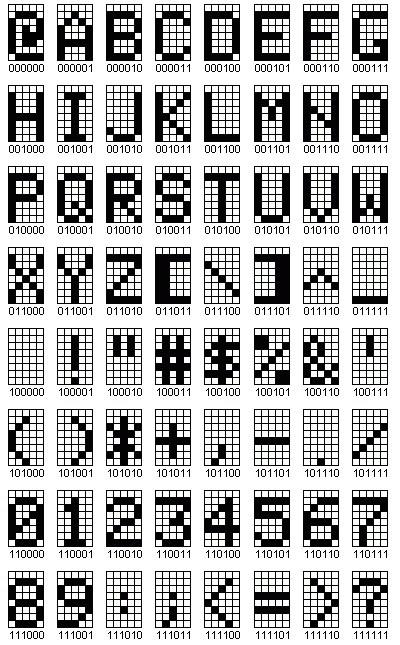
Now we have officially arrived at the character generator ROM IC D2. This is actually no more than a 64 x 7 x 5 bits ROM, in fact it is 64 x 8 x 5 but one of the scan rows can not contain data and is therefore always blank. Thus literally speaking it is a 512 x 5 bit ROM, pre-programmed to contain all 64 possible characters (see diagram below).
The lines A1, A2 and A3 select one of the 8 possible horizontal scan lines.
These 8 scan lines are sequentially stepped through by a simple 3-bit binary counter connected to the 3 input pins.
The lines A4 to A9 are the character select lines, these six inputs select one of the 64 characters to be displayed.
Now you know why we only need a 6-bit wide Video Shift Register.
Since the CE line is permanently tied to ground the 5 outputs of the ROM are constantly outputting the selected bit pattern.
Please note that the character ROM can only generate 64 different characters.
This means that it cannot display lower case characters, nor can it display special characters which are normally generated by entering code below $20.
To drive the character ROM we could simply ignore bit b6, the most significant bit of the normal 128 ASCII table.
This will wrap all upper case characters back to the range of $00 to $1F.
However when we do this the lower case characters will end up in the range from $20 to $3F, which would result in illegible garbage on the screen should lower case characters be printed.
Instead of ignoring ASCII bit b6, we ignore bit b5.
At the same time ASCII bit b6 must be inverted before it is fed to the character ROM.
This way the entire character range from $40 to $7F will end up in the range $00 to $1F (twice of course).
Now lower case characters are automatically translated into their corresponding upper case bit maps.
The characters in the range from $20 to $3F are not affected by this clever little trick because b5, which is "1" for all of them, will be replaced by the inverted b6, which originally is "0" for all of them.
Pixel Shift Register
![]() We can't get enough of shift registers in this description.
Here we've got another one, the Pixel Shift Register IC D1.
Its purpose is to transform the parallel bit pattern on the output of the character ROM into pixels on the screen.
The generated pixels are directly fed into the DA converter (which is a fancy word for 2 resistors, followed by an emitter follower).
The second resistor is driven by a composite sync generator, which combines both Horizontal and Vertical sync pulses into one signal.
We can't get enough of shift registers in this description.
Here we've got another one, the Pixel Shift Register IC D1.
Its purpose is to transform the parallel bit pattern on the output of the character ROM into pixels on the screen.
The generated pixels are directly fed into the DA converter (which is a fancy word for 2 resistors, followed by an emitter follower).
The second resistor is driven by a composite sync generator, which combines both Horizontal and Vertical sync pulses into one signal.
The LD pin copies 8 input bits to the shift register.
But we only had 5 bits coming out of the character generator, where did the other 3 come from?
Simple, they are tied to GND and make sure the characters have some blank space in between them, actually only one of these blank pixels is used.
The CL1 input is the actual pixel clock.
It is half the frequency of the one and only crystal on the board, which is 14.31818 / 2 = 7.1909 MHz.
This clock rate is rather high for an ordinary colour TV screen, which usually doesn't like anything over 5.5MHz.
A black and white TV shouldn't have too much problems with the signal though.
Cursor Control Circuit
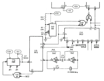 To tell you the truth, I don't really understand all of the Cursor Control Circuit.
This clipping shows you the most important parts of the Cursor Control Circuit.
The seventh 2504 shift register (C11B) is used to store the cursor location, but please don't ask me how, I gave up to do more pleasant things with my spare time :-)
Somehow the signal CURS is generated which is high when the character under the cursor is exposed by the Video Shift Register.
This same signal is fed to gate C12, which normally blocks the square wave which is generated by the NE555 D13.
The output of this gate is connected to gate C10, which toggles the most significant bit to the character ROM whenever the cursor character is displayed.
This toggling results in showing alternately a space character or an "at" symbol.
Please notice that a NOR gate is used for C10, the inverter takes care of inverting ASCII bit b6 like we've discussed in the previous paragraph.
 After some browsing on the internet I found that Steve probably has been inspired by the TV Terminal, designed by